Taiwan Semiconductor Manufacturing Company (TSMC) Chairman Mark Liu on Thursday announced that it would inaugurate its new chipmaking foundry on Japan’s Kyushu island on February 24.
The chipmaking plant has been established as a part of the company’s plan of expansion.
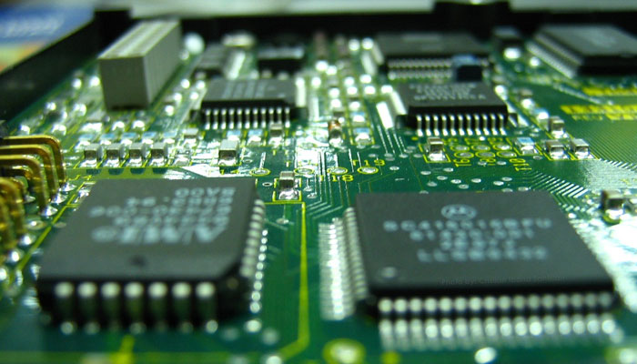
It should be noted that TSMC — whose clients include Apple and Nvidia — controls more than half the world’s output of silicon wafers, used in everything from smartphones to cars and missiles.
In recent years, the company had to navigate geopolitical tussles between the United States and China, as the two have faced off over a range of issues including technology imports, trade and Taiwan — the primary manufacturing base for TSMC.
On Thursday, during an investors call over fourth-quarter earnings, the chairman announced the official date of the long-awaited Japan chip-fabrication foundry´s opening ceremony would be February 24.
"In Japan, we are building a special technology fab in Kumamoto which will utilise 12- and 16-nanometre and 28- and 22-nanometre process technology," Liu said, using industry shorthand to refer to the fabrication foundry.
"We will hold an opening ceremony for this fab on February 24 next month and volume production is on track for the fourth quarter of 2024."
He added that TSMC’s expansion overseas is "based on our customers’ needs and a necessary level of government subsidies for support".
Liu said: "In today’s fractured globalisation environment, our strategy is to expand our global manufacturing footprint to increase our customers´ trust, expand our future growth potential, and reach for more global talents.”
Last year, Japan’s government said it plans to spend $13 billion to boost domestic production of strategically important semiconductors and generative AI technology.


